INTRODUCTION:
They are many DC-DC conversion techniques
available. The most basic technique is linear regulation. However the
efficiency of this technique is very low. Hence switching regulation is used
when higher efficiency is required. The design and working of switching
regulators is complex as they contain non-linear components. Buck-Boost converter
performs same operation as SEPIC but its efficiency is lower when compared to
SEPIC. Hence SEPIC is preferred in high efficiency applications such as
spacecrafts where power losses are critical.
SEPIC gives a constant output when the inputs
are lower or higher or in the range of the constant output. The SEPIC operates
at high efficiency in the range of 90%-95%. Open loop SEPIC has a lower
efficiency when compared to the closed loop SEPIC. However due to some
limitations the open loop SEPIC is not widely used in practical applications.It
is best to use the SEPIC converter with feedback to hold a single output
without the need for control when using a SEPIC as part of a large circuit.
WORKING:
SEPIC configuration provides both buck and
boost action in a single device depending on duty cycle. If the duty is higher
than 50%, then it acts as a boost converter. If the duty cycle is less than
50%, then it works as a buck converter. If the duty cycle is exactly 50%, then
output is same as the input.
Equations:
Duty cycle, D=Vo+Vd/Vin+Vo+Vd
Output voltage, D*Vin/(1-D)
Open
loop SEPIC:

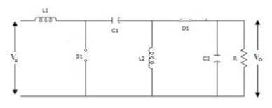
Figure 1: Basic SEPIC circuit diagram
This is the circuit diagram of the basic SEPIC topology.
There are two stages of working i.e. when the MOSFET switch S1 is closed and
when it is open.
When the MOSFET switch is closed:

Figure
2: Open loop SEPIC when the switch is closed
When the switch S1 is closed, energy is stored
in the input inductor L1 and the current through it increases. The voltage drop
across this inductor is equal to the input voltage as the diode D1 is in open
position during this mode. Inductor L2 is charged by capacitor C1. Capacitor C2
discharges through the load, thus giving an output. The equations in this mode
of operation:

When the MOSFET switch is open:
Figure
3: Open loop SEPIC when the switch is open
When switch S1 is open, the diode D1 comes in to play. As the
diode D1 conducts, the input inductor current decreases, charging capacitor C1.
The current through the second inductor L2, decreases linearly to charge the
capacitor C2. The equations in this mode of operation:

MATLAB SIMULINK Circuit:
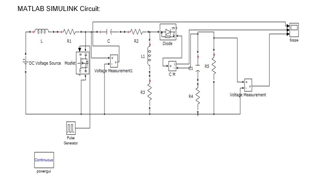
Figure
4: MATLAB SIMULINK open loop SEPIC circuit diagram
Circuit components:
Component
Name
|
Value
|
L1
|
150 microH
|
L2
|
150 microH
|
C1
|
100 microF
|
C2
|
100 microF
|
The resistances R1, R2, R3 and R4 are
parasitic resistances in the order of milli ohms.
The input and load resistance can be
varied as the circuit follows line and load regulation respectively.
Drawbacks:
In open loop SEPIC, there is some ripple current and voltage at the output
which is undesirable. Also, the average efficiency is low when compared to
closed loop SEPIC. However, the main drawback is that the duty cycle should be
varied manually which is not suitable for most of the practical applications.
 |
| Figure 5: shows output voltage and current when input is 10V |
 |
| Figure 6: shows spike in the output volatge and current |
 |
| Figure 7: shows ripple in ouput voltage and current |
No comments:
Post a Comment